


What we think about Applied Materials (AMAT)
Applied Materials in Three Words: Fabrication Equipment Provider
Discuss Applied Materials in our Community Forum
Background
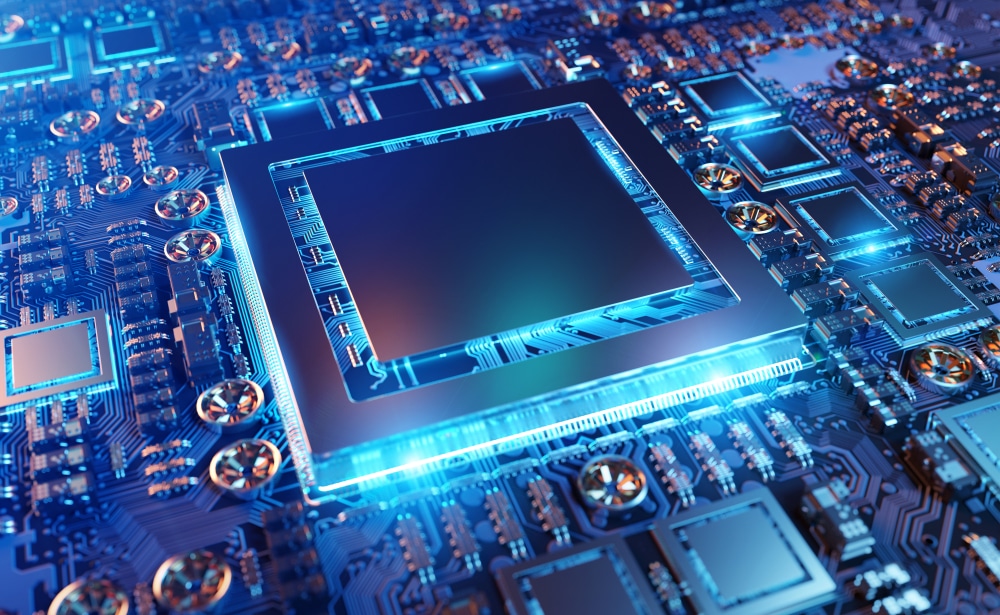
One of the world’s largest wafer fabrication equipment suppliers, Applied provides the precision machinery required to manufacture semiconductor chips. Its deposition, patterning and metrology equipment is what brings innovative chip designs to life.
With over $25 billion in annual sales and an enviable 15% free cash flow margin, it is one of the chip industry’s largest equipment vendors.
The surging popularity of generative AI requires a boatload of computing horsepower to keep up. Regardless of whether companies buy from merchant silicon providers like NVIDIA’s A100 GPUs or AMD’s Epyc CPUs or design their own fit-for-purpose AI chips, they’ll rely on foundries installing Applied Materials’ machinery to get them manufactured and bring them to market.
Applied revealed its new Centura Sculpta pattern shaping machines in early 2023, which would eliminate the need for wafers to go through the EUV lithography process twice. That could turn out to be a significant cost-saver for the entire market, as it’s estimated that lithography accounts for nearly 35% of the overall cost of cutting-edge chips. Applied also took advantage of America’s CHIPS Act to partially fund a new $4 billion state-of-the-art research facility in California.
Applied Materials’ “PPACt playbook” that focuses on superior performance appears to be setting it up for several decades of future growth. Investors can ride the AI tailwind and also enjoy its 0.8% dividend (which it increased 23% this year) and 1.6% buyback yield as its veteran CEO Gary Dickerson leads the company into the next wave of its long-term success.
More recently, “changing chip architectures” are the three most beautiful words for this long-time provider of equipment to the semiconductor manufacturing industry. Moore’s Law has doubled the transistor density of integrated circuits every 18 months for the past 60 years. Now that transistors are commercially produced at just 2 nanometers in width (1/10,000th the size of a human hair), the largest chip manufacturers are forced to adopt new approaches. Samsung’s Gate-All-Around Architecture (GAA), Taiwan Semi’s Nanosheet materials, and Intel’s PowerVia backside power delivery are all new innovations to remain competitive.
Applied Materials is enabling each of these future technology roadmaps with new products of its own, assisting with the deposition, patterning, and metrology required and setting up global innovation centers to work closely with its customers.
Conviction Rating Updates
Applied Materials was upgraded from Buy to Strong Buy on March 12, 2025.
Like many others in the chipmaking equipment industry, AMAT's growth is stuck in neutral. Though its 7% revenue growth here in Q1 2025 is...
Join 7investing (free for your first week!) to get access to this section
Thoughts on Current Valuation and Capital Allocation
Join 7investing to get access to this section
Recent Company Updates:
Join 7investing to get access to this section