Semiconductor manufacturing is getting intensely competitive. Is Taiwan Semi still in the driver's seat?
July 3, 2022
The world’s unquenchable thirst for electronic devices means its demand for chips is going nowhere but up. This semiconductor renaissance has greatly benefited foundry manufacturers like Taiwan Semiconductor (Nasdaq: TSM).
Taiwan Semi has 52% share of the foundry market, meaning it produces the majority of the world’s chips. 52% share qualifies as a quasi-monopoly, where strong IP and capital efficiency advantages serve as barriers to entry to keep smaller competitors at bay.
Yet there are two much larger and vertically-integrated competitors who are also eager to benefit from this semiconductor renaissance. Intel (Nasdaq: INTC) and Samsung offer third-party manufacturing for others as well, and they’re aggressively adding their own new capacity as well. Taiwan Semi has maintained lucrative contracts with heavyweights like Apple (Nasdaq: AAPL), Broadcom (Nasdaq: AVGO), and NVIDIA (Nasdaq: NVDA) for years. But Intel and Samsung would do anything to wrestle those contracts away from them.
One of the most important considerations in semiconductor manufacturing is the intellectual property a company maintains, specifically its process technology. Fabs capable of producing smaller transistors can churn out more densely-packed final circuits that power the cutting-edge devices that need to run a ton of applications simultaneously.
Maintaining process technology leadership has been the heart and soul of Taiwan Semi for decades. There’s a good reason why its business continues to thrive every year, even after spending hardly anything on sales & marketing. TSMC has outspent its rivals by orders-of-magnitude on R&D, relentlessly squeezing every efficiency possible out of Moore’s Law in order to optimize its chip architectures.
Its efforts have paid off. Taiwan Semi has historically derived nearly twice as much revenue per finished wafer as any of its other pure-play, publicly-traded competitors.
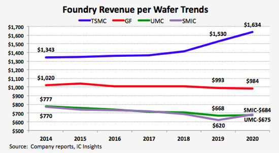
Source: Taiwan Semiconductor Company Update, June 2021
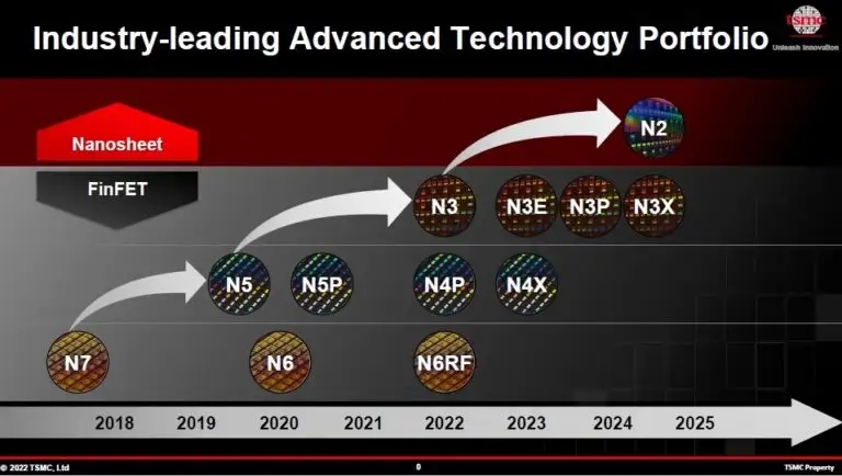
Not content to rest on its laurels, TSMC revealed its forward-looking battle plan at a technical symposium last week. Its technology roadmap includes scaling up its 5 nanometer node technology in its Arizona fab later this year, with commercial chip production from that facility set to begin in 2024. It revealed that its newest 3 nm process tech could also be available later this year, presumably for Apple’s Smartphones or the high-performance computing needs of cloud datacenters.
Both of these process technology improvements are based upon Taiwan Semi’s existing FinFET architecture. The company owns a boatload of patents for this approach and has incrementally been making improvements to make its chips faster and even more power efficient.
Source: SemiWiki.com
Yet Taiwan Semi also revealed something new this month. It announced that its latest-and-greatest 2 nm process tech would be based on a new nanosheet architecture, which is straying from the course of what it’s traditionally done. TSMC believes its nanosheet designs will be even more efficient, showing either a 10-15% speed increase at the same power or a 25-30% power reduction at the same speed.
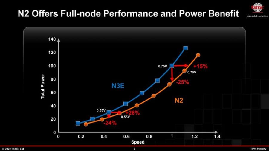
Source: Taiwan Semiconductor Technical Presentation
This is innovation at its finest. TSMC is capturing every efficiency possible out of its proprietary technology. But it also isn’t afraid to disrupt its traditional approach and make drastic improvements in order to unlock new research improvements.
TSMC’s research also isn’t taking place in a vacuum. Samsung and Intel are showcasing their own technology roadmaps, which they hope will appeal to Taiwan Semi’s demanding customers.
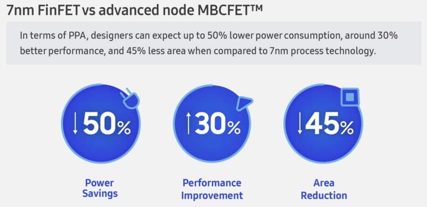
Samsung unveiled its own 3 nanometer Gate All Around technology (GAAFET), which it thinks could be ready later this year. Samsung claims its 3nm GAA tech would provide 50% less power consumption, 30% better performance, and take up 45% less space than existing 7nm process technologies; which is a clear shot across the bow of TSMC’s 7nm FinFET tech.
Source: Tom’s Hardware
Intel had a few things to show off as well with its own three-year roadmap. Intel’s somewhat-new-yet-also-somewhat-legendary CEO Pat Gelsinger has adopted ASML’s extreme ultraviolet lithography approach and is ready for his company to become a best-in-class foundry services provider. Intel’s roadmap claims it will have EUV implemented into its fabs by late 2022 (Intel 4) and will have process technology that is commercially competitive with all of its peers within three years. Its technology leadership by 2025 call for it to embrace ASML’s (Nasdaq: ASML) newest high-NA technology to manufacture sub nanometer transistors.
In a nutshell, Gelsinger is aggressively stepping on the Intel accelerator. He’s going all-in on R&D and is ready to go head-to-head with TSMC for the most lucrative customer bids.
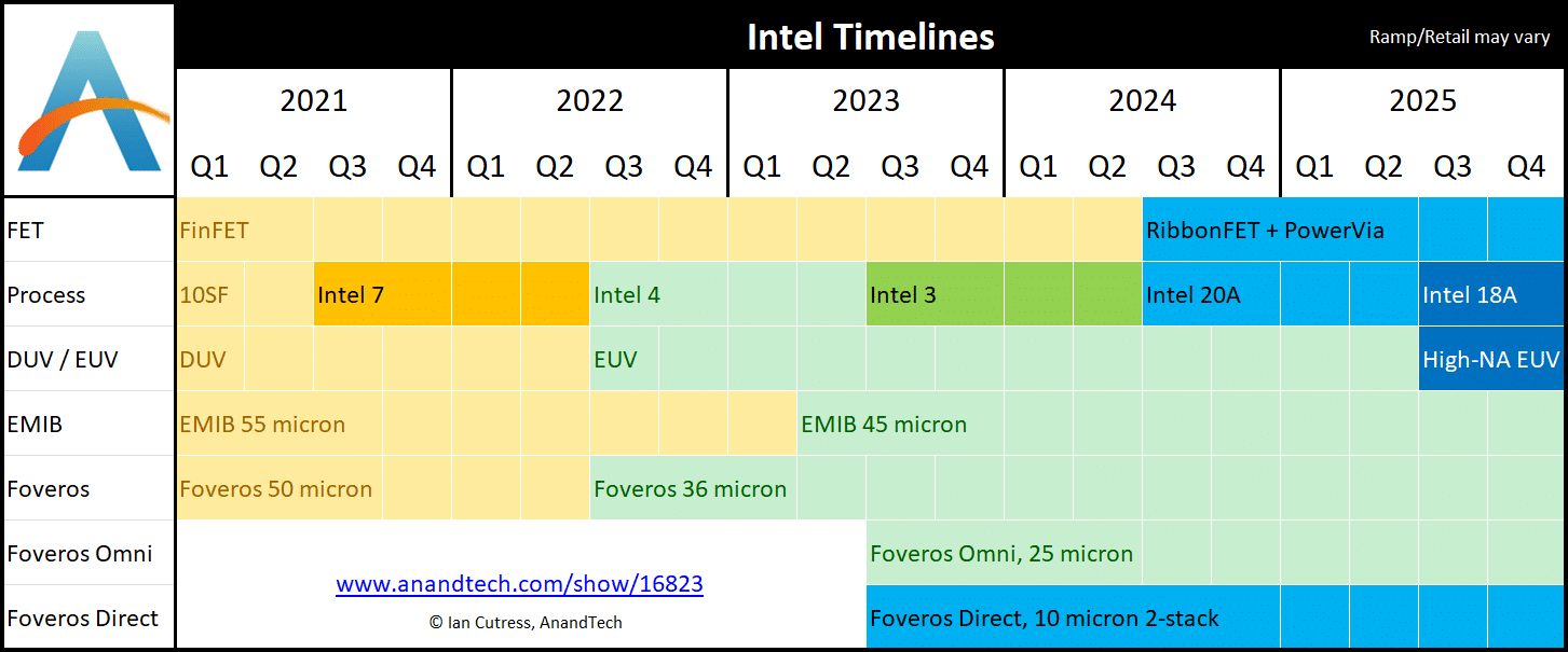
Source: AnandTech
Of course, these are all just strategic plans. Now it comes down to the execution. The semiconductor industry has complex supply chains that span across continents. The ultimate winners of the semiconductor renaissance will perfectly marry research, development, operations, and financial efficiency.
We’re in the middle of a three-way dogfight to produce the world’s most cutting-edge chips. Taiwan Semi’s rise to the top was assisted by Samsung’s Vice Chairman being imprisoned for embezzlement and Intel’s stubborn refusal to embrace EUV from the start.
There’s no shortage of demand for chips to power the next generation of Smartphones, high-performance data centers, the Internet of Things, and autonomous vehicles. And the stakes are getting too high to get left behind.

Already a 7investing member? Log in here.